Power-off laser fault injection on embedded security primitives
- Project Type: Internship hardware security
- Tools: Python, laser laboratory sources (picosecond, nanosecond)
- Duration: 4 months
- Team: SAS department EMSE
Introduction
This internship aims to investigate whether power-off laser fault injection can be utilized to disable or manipulate security mechanisms, such as Physically Unclonable Functions (PUFs) or Bulk Built-In Current Sensors (BBICS).
The project will focus on designing experiments and testing them on a specialized chip, which is used to simulate the effects of radiation on a system.
Project Overview
The project involves:
- Understanding the different physical attacks on chips
- Exploring the use of laser to induce faults on devices
- Developing experiments aimed at influencing security sensors
- Analyzing results for security evaluation
Important Definitions
BBICS (Bulk Built-In Current Sensors)
Bulk Built-In Current Sensors are essential components used in modern embedded security systems to:
- Detect current anomalies in the bulk substrate of integrated circuits, specifically when subjected to external attacks like laser fault injection.
- Generate an alert flag, triggering an alarm whenever an anomaly or fault condition is detected, thus preventing potential breaches or malfunctions in the chip.
- Operate by sensing transient currents within the CMOS structure, helping to maintain system integrity during fault conditions.
BBICS play a critical role in securing integrated circuits against physical attacks, such as power-off laser fault injection. By ensuring that any suspicious activity is flagged, these sensors protect sensitive data and security mechanisms in embedded systems.
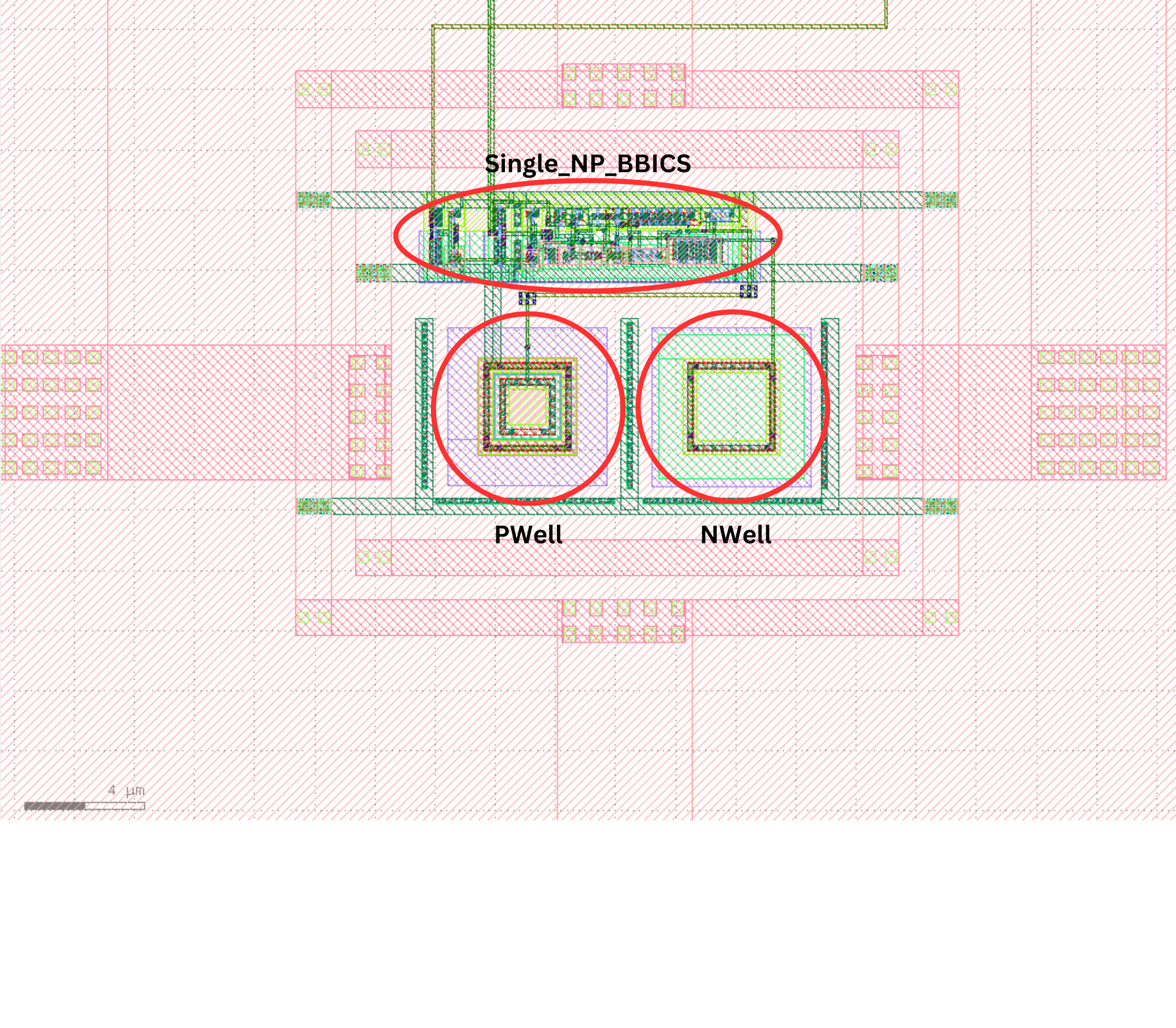
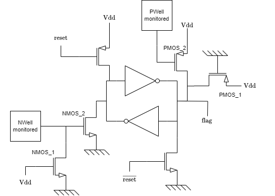 Figure 1: Architecture of a single NP BBICS
BBICS are composed of a latch in the middle, and are surrounded by transistors connected to N-wells and P-wells on either side. When a transient current is detected in the bulk, the transistors trigger a change in the state of the latch, which raises an alert signal. This configuration ensures the detection of anomalies in both N-type and P-type regions, maintaining comprehensive fault detection coverage in the CMOS structure.
Single Event Effects
Single Event Effects (SEEs) occur when an ionizing particle strikes a sensitive node within a semiconductor device, altering its state. This impact can lead to errors in digital circuits or transient faults in memory cells, known as Single Event Upsets (SEUs). According to NASA’s definition, SEEs are measurable effects on a circuit caused by ion impact. These effects include, but are not limited to:
- Single Event Upset (SEU): A transient state change induced by an energetic particle, affecting components like digital, analog, or optical elements. SEUs are "soft" errors that can be corrected by resetting or rewriting the device.
- Single Event Transient (SET): A temporary incorrect output caused by a transient current, induced by an ionizing particle striking a PN junction. This type of event does not permanently alter the device, but the erroneous output can lead to security vulnerabilities.
- Single Event Latchup (SEL): A persistent short-circuit state triggered by an ionizing particle, which often requires a power cycle to correct.
- Single Event Burnout (SEB): A catastrophic failure where an ionizing particle induces a high-current state, leading to permanent destruction of the device.
- Single Event Gate Rupture (SEGR): A physical rupture of the gate oxide in a MOSFET due to ionizing particle impact.
- Single Event Dielectric Rupture (SEDR): A rupture in the dielectric layer of a semiconductor device caused by an ionizing particle, which can result in permanent damage.
Example on a CMOS inverter:
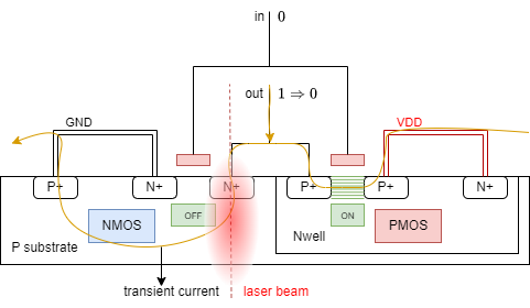
Figure 2: Inverter with input '0'
This diagram illustrates the behavior of an inverter circuit when a Single Event Transient (SET) induced by a laser occurs, with the input set to '0'. In this state:
- Input and output states: The input of the inverter is '0', which means the NMOS transistor is off and the PMOS transistor is on. As a result, the output is '1'.
- Laser impact: A laser beam hits the NMOS transistor, causing a transient current.
- Effect of the transient current: This transient current can induce a SET, potentially changing the output state from '1' to '0'.
- Sensitive regions: The sensitive region in this scenario is the NMOS transistor, which is vulnerable to the transient induced by the laser when the input is '0'.
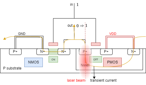
Figure 3: Inverter with input '1'
This diagram illustrates the behavior of an inverter circuit when a Single Event Transient (SET) induced by a laser occurs, with the input set to '1'. In this state:
- Input and output states: The input of the inverter is '1', which means the NMOS transistor is on and the PMOS transistor is off. As a result, the output is '0'.
- Laser impact: A laser beam hits the PMOS transistor, causing a transient current.
- Effect of the transient current: This transient current can induce a SET, potentially changing the output state from '0' to '1'.
- Sensitive regions: The sensitive region in this scenario is the PMOS transistor, which is vulnerable to the transient induced by the laser when the input is '1'.
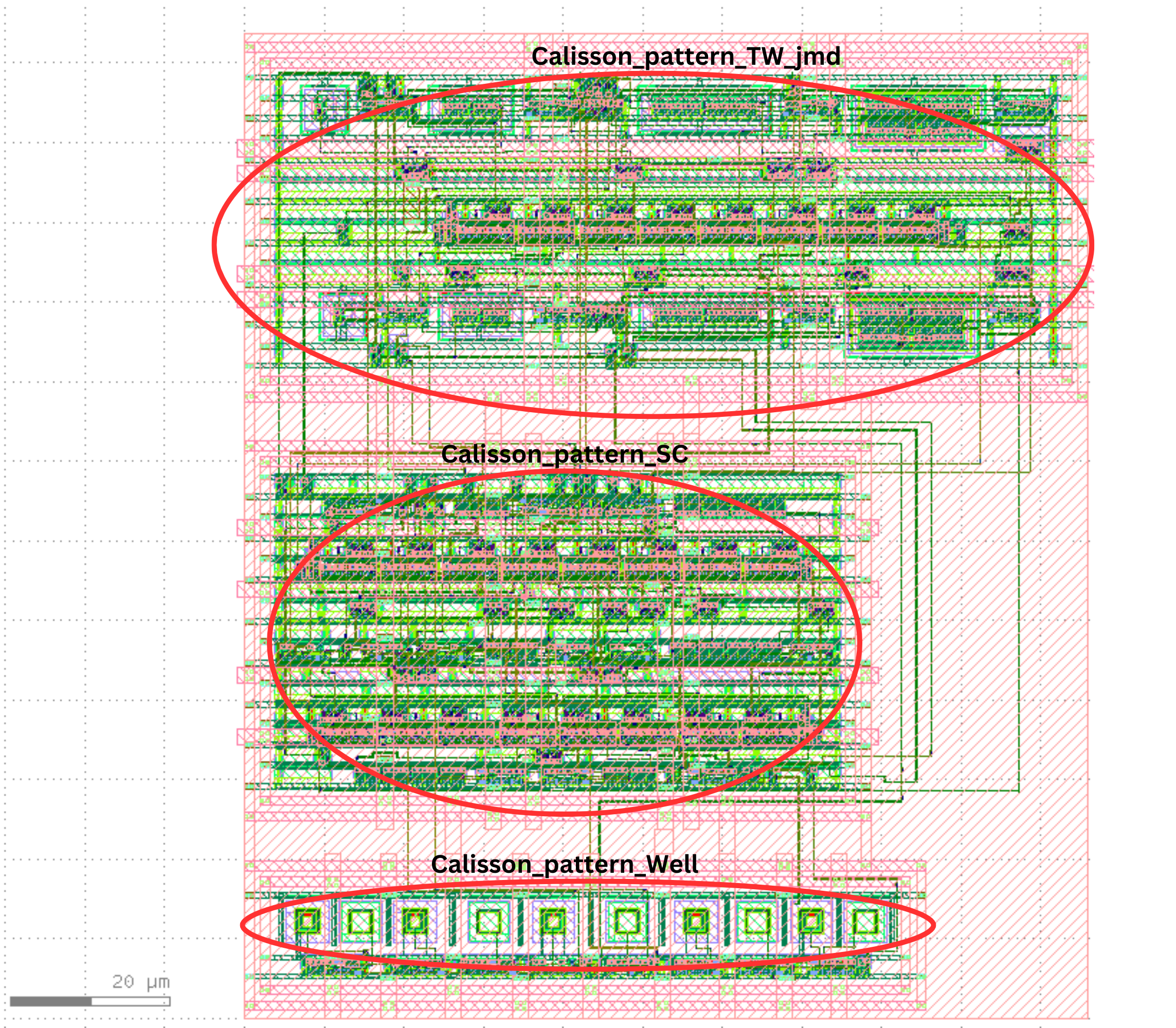
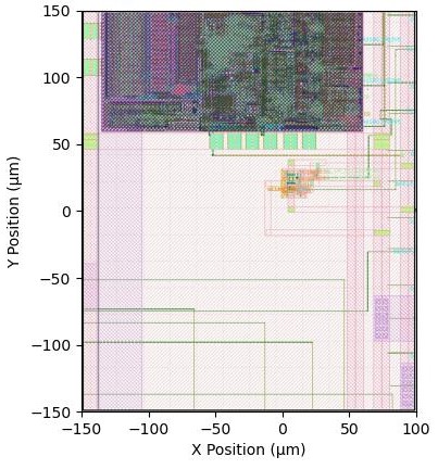
Layout Analysis (GDS File) of the Radhard Chip
Since the chip we are working on is the result of research from the SAS laboratory, we have access to the layout files of the Radhard board (Radiation Hardening). This allows us to know where to direct our efforts. In our case, we will first focus on the single_BBICS located at the top of the board, and then on the Calisson_pattern_Well block, which is located at the bottom of the pattern_SC_TW_Well block and groups together the different BBICS with high sensitivity (hs_bbics) and low leakage (ll_bbics).
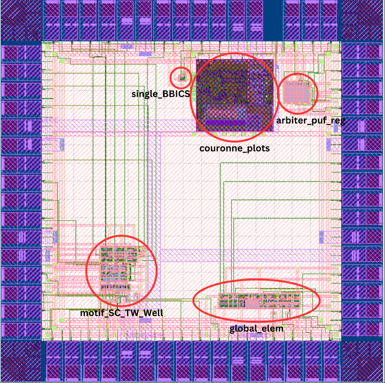 Figure 4: Complete layout of the Radhard board
Layout of the isolated single BBICS
Layout of the BBICS block
 Figure 5: Zoom on the layout of the single BBICS
BBICS Functionality Verification
To verify the functionality of the BBICS, we first perform characterization at different laser energies and pulse widths.
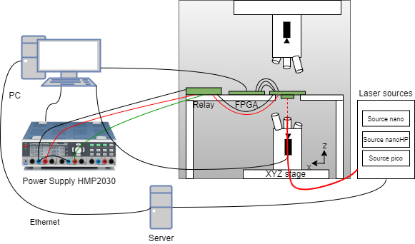
To achieve this, we used the following experimental setup:
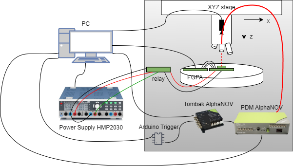 Figure 6: Experimental setup for BBICS characterization
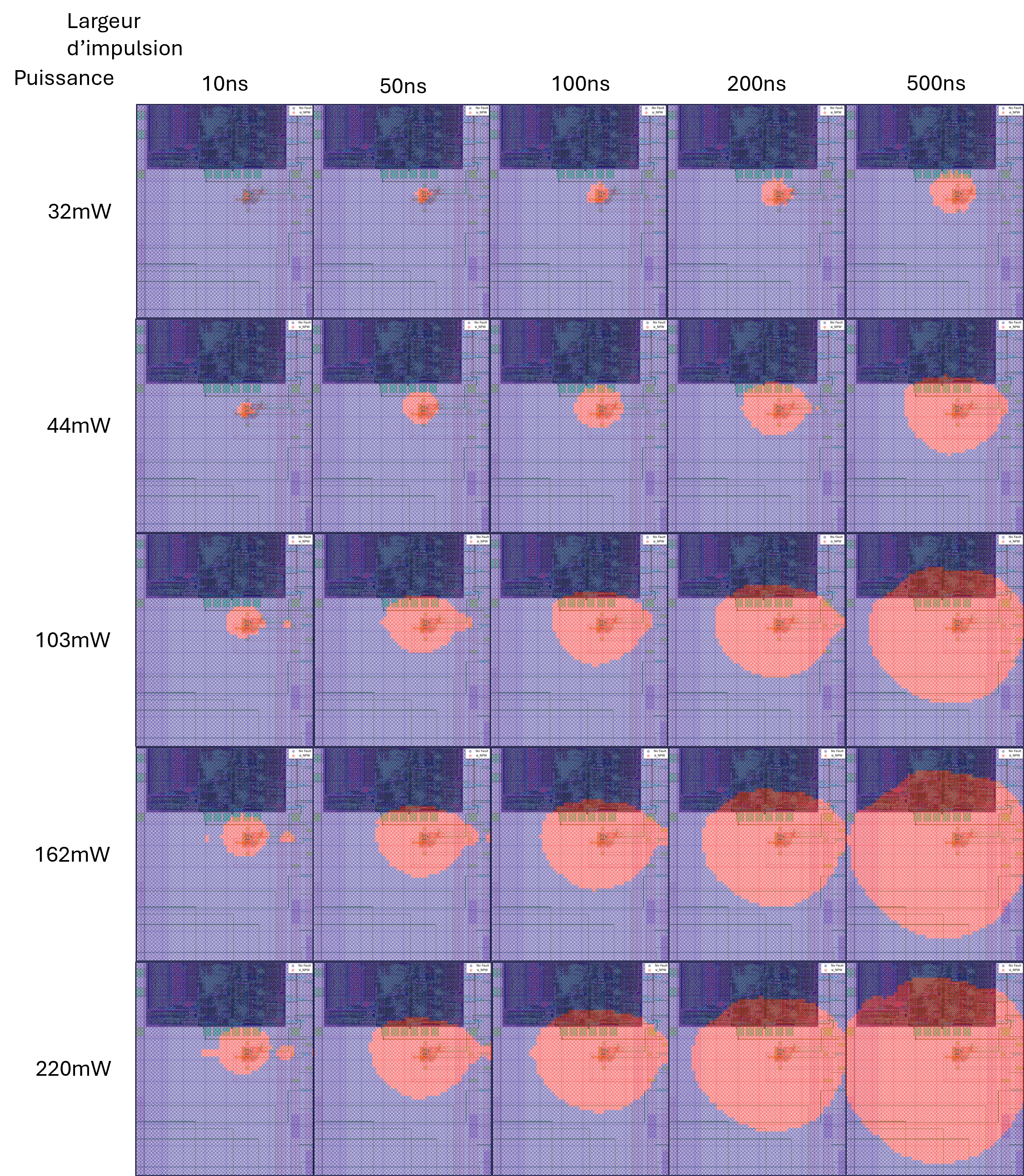
The camera provides real-time information on the laser’s position during the attack, allowing us to precisely target the desired BBICS with the help of the layout shown in the figure below.
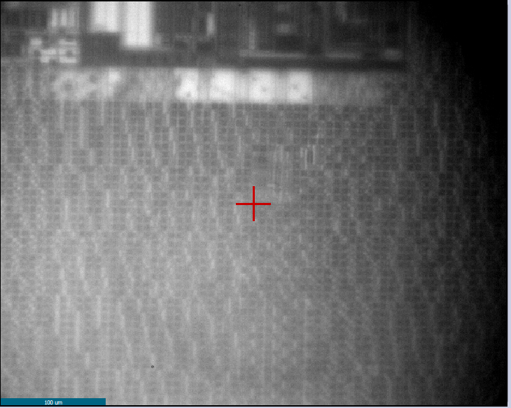
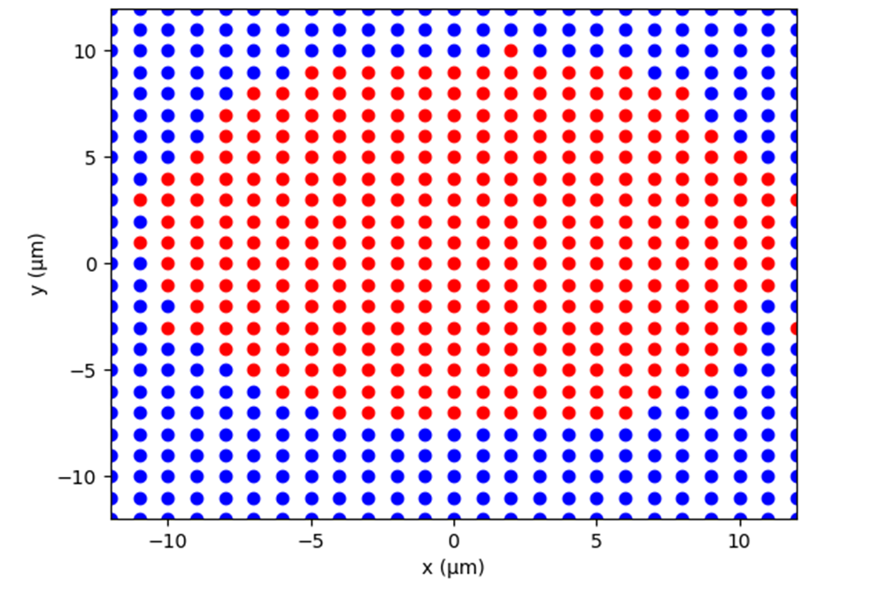
Location of the origin (0,0) for the attack on the single BBICS
Characterization zone on the Radhard.gds layout (characterization 4)
Summary of Characterization Parameters
Here are the parameters used to characterize the operation of the BBICS. The table below lists the different ranges of the laser attack, the step size, the maximum current sent to the optical fiber, and the pulse width.
| № | Range (x,y) [\(\mu m\)] | Step \(\Delta\) [\(\mu m\)] | \(I_{max}\) [mA] | PW [ns] |
|---|---|---|---|---|
| 1 | (-50,-50) → (75,75) | 5 | 75, 100, 200, 300 | 5, 10, 50, 100, 200, 500 |
| 2 | (-20,-20) → (45,45) | 0.5 | 50, 75, 100 | 5, 10, 50, 100, 200, 500 |
| 3 | (-50,-50) → (75,75) | 5 | 60, 70, 80, 90, 100 | 10, 50, 100, 200, 500 |
| 4 | (-150,-150) → (100,150) | 5 | 80, 100, 200, 300, 400 | 10, 50, 100, 200, 500 |
| 5 | (-30,0) → (70,70) | 1 | 100, 200, 300, 400, 500, 1000 | 5 |
Table 1: Characterization
Results of the characterization
Characterization on the Calisson_pattern_Well Block
We also performed a characterization on the block containing the other BBICS, although these are not the ones we will attack first.
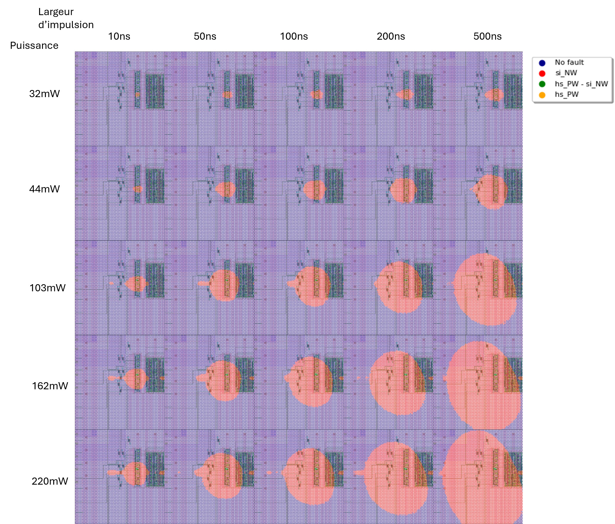
We can already observe two surprising results from these characterizations:
- Only 4 flags are present (no fault, single NWell, high sensitivity PWell, and both at the same time).
- The high sensitivity BBICS seems to detect fault injections less sensitively than the single NWell BBICS.
My mistake here was only performing one characterization. Indeed, the result does not seem to be consistent, and we cannot be sure of the proper functioning of the other BBICS. I should have run a characterization on another test card to compare the results.
Attack protocol
Several aspects need to be tested with different parameters to try to temporarily or permanently damage our integrated mass current sensor.
First, the initial idea was to attack in order to exceed the TID (Total Ionizing Dose) of the targeted area. Indeed, when using a pulsed laser, it generates radiation effects that, at certain doses, can modify the behavior of the electronic circuit either temporarily or permanently. These radiation effects stem from the interactions between the laser and the sensor material, generating electron-hole pairs and inducing parasitic currents. As the accumulated radiation dose increases, these currents can alter the electrical characteristics of the components, leading to malfunctions. For example, a sufficient dose of radiation can cause a threshold voltage shift in transistors, an increase in leakage current, or a degradation of the overall performance of the circuit. These changes can result in temporary malfunctions, where the sensor can recover after a certain time, or permanent malfunctions where the damage is irreversible.
Next, the second way to attack the integrated mass current sensor would be to use thermal effects associated with pulsed laser attacks, thus melting certain transistors during the attack.
The experimental protocol I devised for these two methods is as follows:
- Initial rough characterization (BBICS on)
- Turning off the board’s power supply
- Attack with energy/power P for X seconds and at a frequency F
- Powering the board
- Final rough characterization (BBICS on)
These attacks will be performed using two different laser sources (nanosecond and picosecond) to test the different effects related to these sources.
The first targeted attacks we conducted on the BBICS were carried out on a different setup than the one used during the characterization (see Figure below). This setup uses the advanced laser from room E017, which has several interchangeable laser sources (nanosecond source, high-power nanosecond source: NanoHP, and a picosecond source).
This laser allowed us to carry out our experimental protocol with the greatest number of possible parameters (see tables below).
Summary of the attacks performed with the picosecond laser source:
| Attack Name | Energy [nJ] | PW [ps] | Optics | Frequency F [Hz] | Time T [s] |
|---|---|---|---|---|---|
| exp_pico1 | 1 → 50 | 30 | x20 | continuous (1 MHz) | 180 → 300 |
| exp_pico2 | 50 | 30 | x20 | continuous (1 MHz) | 180 → 300 |
| exp_pico3 | 10 → 45 | 30 | x20 | continuous (1 MHz) | 180 → 600 |
Table 3: Attacks performed with the picosecond source
Results
Nanosecond Source
Summary of Results:
All attacks using the nanosecond laser source (experiments exp1 to exp17) were unsuccessful in causing damage or detectable effects on the BBICS. Comparisons of the sensor’s performance before and after the attacks showed no significant changes, meaning the sensors continued to function as before.
Challenges Faced:
Increasing the attack duration might have led to more significant effects, but the laser would often overheat and shut down when performing consecutive attacks or extended attacks, especially in the final experiments (exp8 to exp17) where high power and long durations were used.
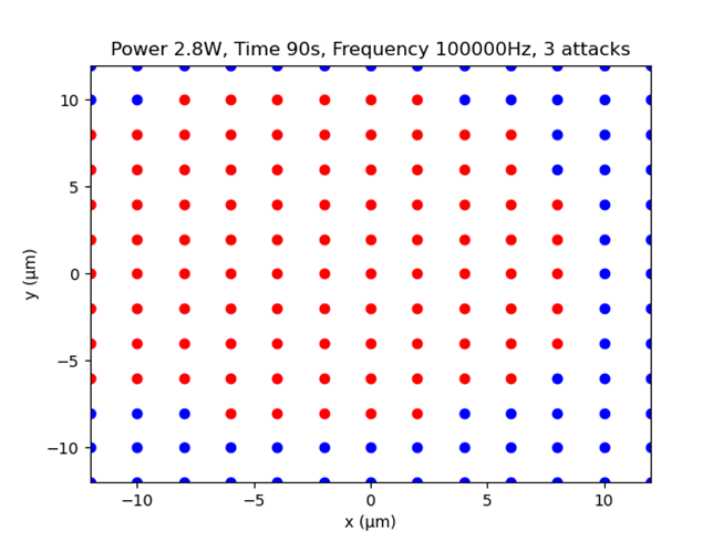
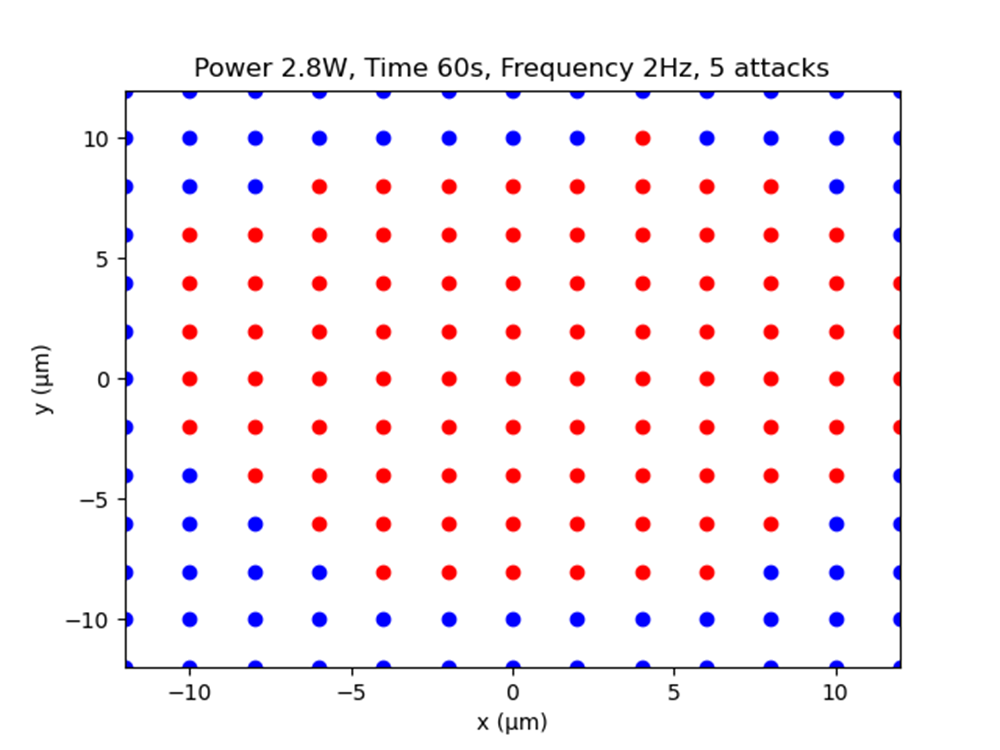
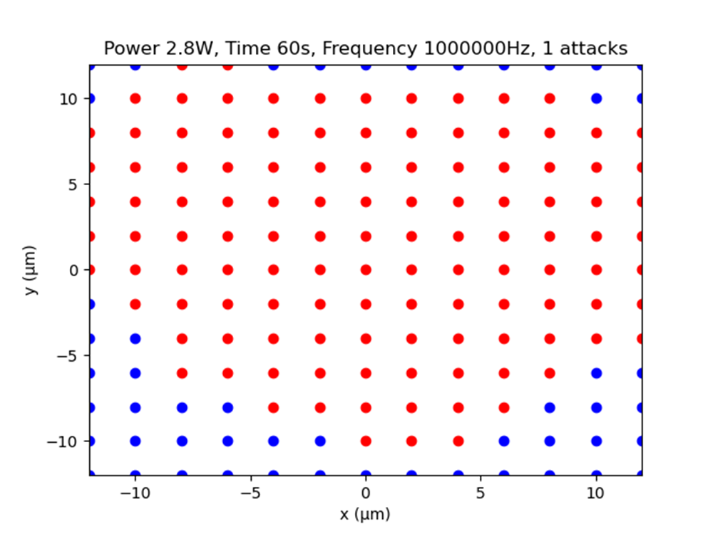
Visuals:
- Figure 1: Initial characterization with the nanosecond laser source (10 mW at 50 ns, x20 optics)
- Figure 2: Experiment exp6 (2.8W - 500ns - 90s)
- Figure 3: Experiment exp8 (2.8W - 1s - 60s)
- Figure 4: Experiment exp17 (2.8W - 500ns - 600s)
Picosecond Source
Results:
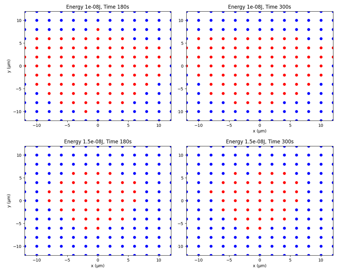
For the picosecond source, we obtained better results. We gradually increased the attack energies from 1 nJ to 50 nJ, while testing for various durations ranging from 180 to 300 seconds.
The first attack (exp_pico1) already shows that the attacks have a short-term effect on the detection range of the BBICS. Indeed, as the energy increases, we notice that the detection threshold of the BBICS gradually decreases.
Influence of Duration:
Based on the results, the attack duration does not seem to have a significant influence on the detection threshold.
Visuals:
- Figure 5: Comparison of attack results from 10 nJ to 15 nJ for 180 and 300 s (characterization done at 0.1 nJ and 30 ps)
As the energy of the attack increases, this reduction in the detection range of the transient current sensor becomes more pronounced. These results, obtained with the picosecond laser, support the idea that it is possible to conduct an attack that could permanently or temporarily bias the sensor. After a certain time, the BBICS would return to its normal detection threshold.
Another step in the analysis, which I did not have time to conduct, would be to measure how long it takes for the sensor to return to its initial state after an off-power attack.
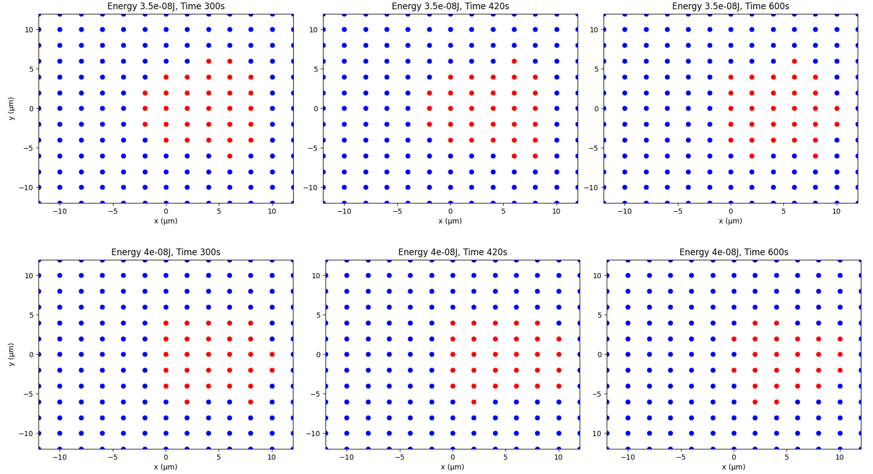
Higher Energy Attacks:
New attacks with higher energy were conducted. In Figure 6, we can see the characterizations done after attacks with 35 to 40 nJ. In this energy range, the reduction in the detection range is not as obvious as between 10 nJ and 15 nJ, but it remains present.
Finally, by increasing the energy further, we achieved a permanent BBICS failure for an energy of 45 nJ during a 300-second attack. The first attack that permanently biased the BBICS was performed with 50 nJ for 180 seconds and was confirmed by another attack at 45 nJ for 300 seconds on a different board.
Visuals:
- Figure 7: BBICS attack at 50 nJ 30 ps on board number 4
- Figure 8: BBICS attack at 45 nJ 30 ps on board number 6